The GPU Hardware Model
CUDA Deep Dive · Part 1: CUDA Foundations · B-02
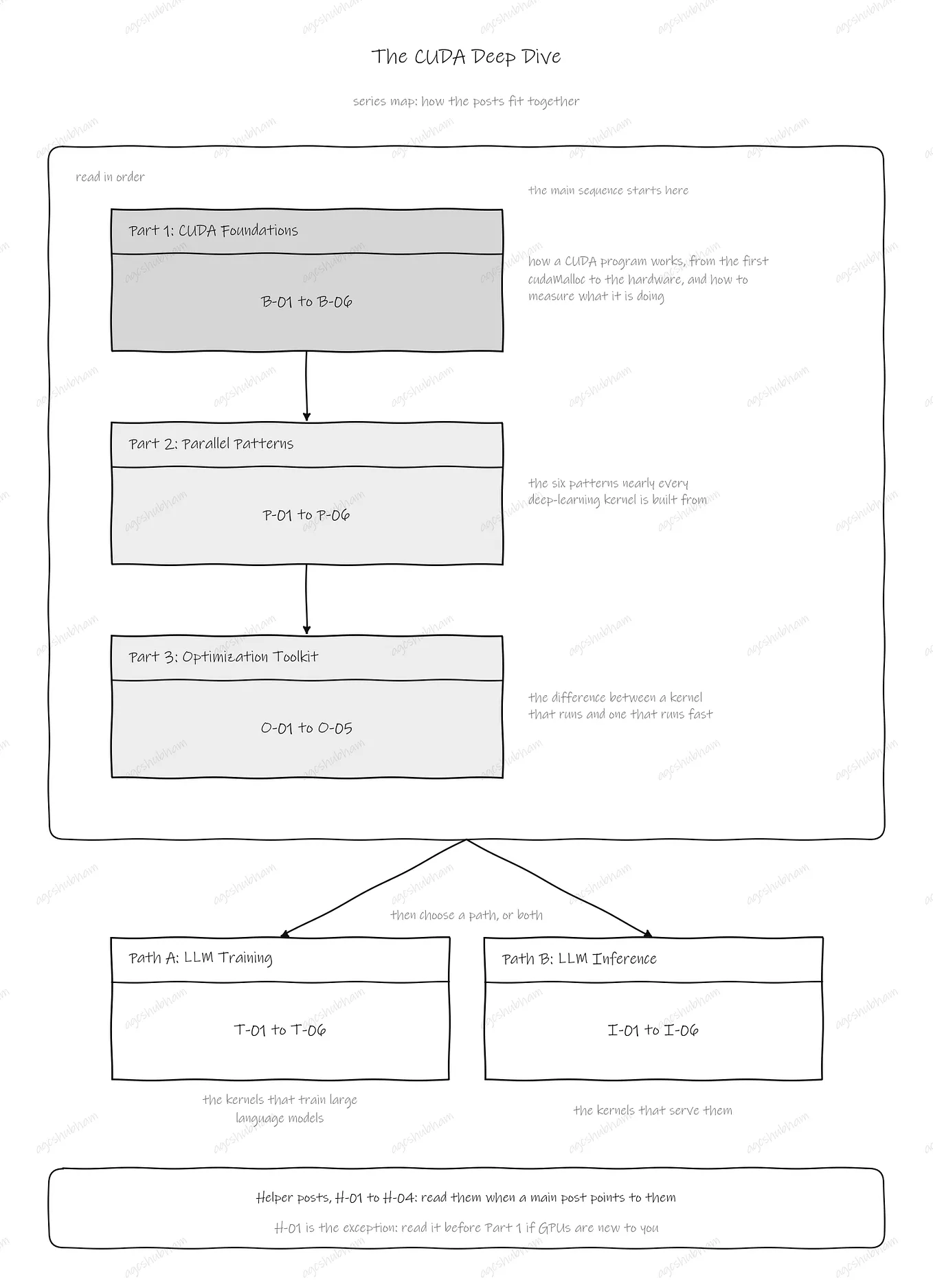
This post is one of a series. See the Series Map for the full plan and where this post fits. Previous: B-01 The CUDA Program Lifecycle. Next: B-03 Memory Hierarchy Deep Dive (coming soon).
What the GPU does with the 4,096 blocks that B-01 launched: SMs, warps, divergence, registers and the memory wall, explained one piece at a time.
Who this is for: a software engineer or ML practitioner who knows C++ basics (pointers, stack vs heap, manual memory allocation), may have used PyTorch, and has never written a CUDA kernel.
What this post does: it explains what the GPU did with the kernel B-01 launched. What an SM is. How a block becomes warps. What a warp costs when its 32 threads disagree. Why registers decide how many threads fit on an SM. And why memory bandwidth, not arithmetic, sets the speed of most kernels. By the end you have a model of the chip that the rest of the series builds on.
Start here if you have run one kernel and want to know what the GPU did with it. If you have not, read B-01 The CUDA Program Lifecycle first; it is the program this post takes apart. If GPUs themselves are new to you, read H-01 Why GPU? CPU vs GPU Architecture first: it explains why the chip is built this way, and this post only explains how.
Where B-01 left off
B-01 followed one program from start to finish. Its kernel launch was this line: vectorAdd<<<4096, 256>>>(...). The first number is how many blocks, 4,096. The second is how many threads each block has, 256. Together that is 1,048,576 threads, one per element of the vectors. B-01 stopped at the point where the GPU takes those blocks. This post picks up there.
Here are the four facts this post is about. A GPU is built from a small number of identical processing units called streaming multiprocessors, or SMs. The GPU gives each block to one SM, and that SM runs it. Inside the SM, the block’s threads do not run one by one; they run 32 at a time, in groups called warps. And there are far fewer SMs than blocks, so each SM works through a few blocks at once while the rest wait their turn.
H-01 explained why a GPU is built this way. The short version: a CPU core uses its transistors to finish one instruction stream as fast as possible. A GPU uses the same transistors for many simple arithmetic units and for moving large amounts of data at once. This post shows where those transistors went on the chip, and what that layout means for your kernel.
If there is one sentence to keep from the whole post, it is this:
The GPU never runs one thread by itself. It runs 32 threads at a time, as a warp. It hands out registers and shared memory per SM. And for most kernels, memory delivers bytes more slowly than the SMs can use them.
The post has six parts. First, the whole chip: what an SM is and what all the SMs share. Second, the inside of one SM. Third, how a launch is split into blocks, warps and threads, and how many blocks one SM can run at the same time. Fourth, how an SM runs one warp, and what happens when its 32 threads disagree. Fifth, the memory wall: why most kernels wait for memory, not for arithmetic. Sixth, Tensor Cores, and a short list of what newer GPUs add. Figure B02.1 is the picture of the whole chip that the first part describes.
Figure B02.1: A GPU is many identical SMs sharing one L2 cache and one device memory, and a grid is almost always bigger than the GPU can hold at once

A GPU is many identical SMs
In B-01 the GPU was one box that the CPU sends work to. Inside the box, the first thing to notice is that one unit is repeated many times. A GPU is a row of identical processing units called streaming multiprocessors, or SMs. A laptop GPU has a few dozen SMs at most. Large data-centre GPUs have more than a hundred. Every SM has the same arithmetic units, the same scheduling hardware and the same private memory. No SM is special. A bigger GPU is a GPU with more SMs. A program that runs well on a GPU is a program that gives every SM something to do.
Three things on the chip are shared by all the SMs.
- The L2 cache. One cache that sits between the SMs and the memory. If one SM has recently fetched a value, another SM can get it from the L2 without going out to memory. You do not control the L2. It is just there.
- The memory controllers and the device memory. Device memory is the VRAM on the card. It is the memory that
cudaMallocreserved andcudaMemcpyfilled in B-01. Every SM reads and writes it through the same set of memory controllers. That is why memory bandwidth, the number of bytes per second the memory can deliver, is a property of the whole GPU and not of any one SM. It is the number this post comes back to most often. - The PCIe link. The connection back to the CPU. B-01 was about moving data across it. This post is not. Once the data is on the card, PCIe plays no part.
Now the placement rules. The rest of the post depends on them.
- When you launch a kernel, the GPU hands its blocks out to the SMs.
- A block runs on one SM for its whole life. It never moves to another SM and never spans two.
- One SM runs several blocks at the same time, up to limits we will calculate below.
- The threads of one block can share their SM’s private memory and can wait for each other, because they are on the same SM. Threads in different blocks cannot, because they may be on different SMs. B-03 and P-02 build
__shared__memory and__syncthreads()on this rule.
If a picture helps: think of a factory with a few dozen identical workstations. A block is a team of workers sent to one workstation for one job. A workstation can host several teams at once. Teams at different workstations cannot talk to each other.
Since every SM is the same, the next question is what one SM contains.
Inside one SM
An SM has four kinds of hardware. Every kernel uses all four, whether or not it knows it.
- Warp schedulers and arithmetic lanes. An SM is divided into a few partitions, four on current designs. Each partition has one warp scheduler and a group of arithmetic lanes. In every clock cycle the scheduler picks a warp that is ready and issues that warp’s next instruction. The lanes carry the instruction out, one lane per thread. The lanes are what product sheets call CUDA cores. The fact to hold on to: a scheduler issues one instruction for 32 threads at a time. The next two sections build on it.
- The register file. One pool of 65,536 registers per SM. Each register is 32 bits, so the pool is 256 KB. Every thread running on the SM gets its registers from this one pool. A thread’s local variables live in its registers. A thread keeps its registers from the moment its block arrives on the SM until the block finishes.
- Shared memory and L1 cache. One piece of fast memory on the SM itself. Part of it works as an ordinary cache, the L1. The rest is shared memory: a scratchpad that all the threads in one block share. Depending on the GPU, an SM has somewhere between 64 KB and a few hundred KB of it. B-03 is about using it well.
- Load/store units, special function units and Tensor Cores. The load/store units turn a thread’s memory read or write into a request to the L1, to the L2 or to device memory. The special function units compute things like square roots and exponentials that would be slow on the ordinary lanes. The Tensor Cores multiply small matrices in a single instruction. The last section comes back to them.
You do not have to take these numbers from a specification sheet. The CUDA runtime can describe the GPU it is running on. This program prints the parts of that description this post uses:
#include <cuda_runtime.h>
#include <cstdio>

int main() {
    cudaDeviceProp p;
    cudaGetDeviceProperties(&p, 0);
    printf("device name           %s\n", p.name);
    printf("SMs                   %d\n", p.multiProcessorCount);
    printf("warp size             %d\n", p.warpSize);
    printf("max threads per SM    %d\n", p.maxThreadsPerMultiProcessor);
    printf("max threads per block %d\n", p.maxThreadsPerBlock);
    printf("max blocks per SM     %d\n", p.maxBlocksPerMultiProcessor);
    printf("registers per SM      %d\n", p.regsPerMultiprocessor);
    printf("shared memory per SM  %zu KB\n", p.sharedMemPerMultiprocessor / 1024);
    printf("shared mem per block  %zu KB\n", p.sharedMemPerBlock / 1024);
    printf("L2 cache              %d KB\n", p.l2CacheSize / 1024);
    printf("device memory         %zu MiB\n", p.totalGlobalMem >> 20);
    return 0;
}
Save it as devquery.cu, build it with nvcc -arch=native -o devquery devquery.cu, and run it. Every line it prints is a property of your particular GPU, and two GPUs rarely agree on all of them. The structure behind the numbers is the same on every CUDA GPU.
So that the arithmetic in this post has concrete numbers to work with, it uses an example GPU. It is not a real product, just round numbers of the kind the query prints: 32 SMs, a warp size of 32, 2,048 threads per SM, 1,024 threads per block, 32 blocks per SM, and 65,536 registers per SM. Three of these do most of the work in what follows: 32 SMs, 2,048 threads per SM, and 65,536 registers per SM. Run the query on your own GPU and substitute your numbers; every calculation below works the same way. Figure B02.2 draws one SM.
Figure B02.2: An SM is a few warp schedulers, 65,536 registers and one shared scratchpad, and everything a block uses comes out of them

The SM is fixed. The launch is what you choose. The next section is about how a launch is cut up to fit the SM.
How a launch is split up: grid, block, warp, thread
B-01’s launch asked for 4,096 blocks of 256 threads. You chose both numbers, and you can change them. The grid (how many blocks) and the block (how many threads in each) are yours.
The warp is not yours. It belongs to the hardware. When a block arrives on an SM, the SM splits its threads into groups of 32 by threadIdx.x. Threads 0 to 31 make warp 0, threads 32 to 63 make warp 1, and the pattern continues to the end of the block. A block of 256 threads is eight warps. There is no place in the launch syntax to ask for a warp, and the hardware never schedules anything smaller than one.
Because the split is always 32 wide, every block is rounded up to a multiple of 32 lanes, whether or not you asked for one. Say you launch blocks of 33 threads. Each block becomes two warps. The first warp is full. The second has one live thread and 31 empty lanes. Those 31 lanes are not free. They hold registers, they take their turn in the scheduler like any other lane, and they produce nothing. A block of 200 threads is seven warps, which is 224 lanes, with 24 lanes empty in the last warp. That is about one lane in ten wasted. Figure B02.3 shows the split and the waste for several block sizes. B-04 turns this into the rule for choosing a block size. Here the point is to see why the rule exists.
Figure B02.3: A 256-thread block is eight warps, cut in threadIdx order, and any block size is padded up to whole warps

Two and three dimensions. A block or a grid can have two or three dimensions. This is a convenience for data that has two or three dimensions: an image, a matrix, a volume. The type for this is dim3. Here is a kernel and a launch that touch every pixel of a 28 x 28 image using 16 x 16 blocks:
__global__ void touch(float* img, int width, int height) {
    int col = blockIdx.x * blockDim.x + threadIdx.x;
    int row = blockIdx.y * blockDim.y + threadIdx.y;
    if (row < height && col < width) {
        img[row * width + col] += 1.0f;
    }
}

dim3 block(16, 16);
dim3 grid((28 + 15) / 16, (28 + 15) / 16);   // 2 x 2 blocks
touch<<<grid, block>>>(d_img, 28, 28);
Two things to notice.
First, the rounding-up division from B-01 happens in each dimension, and it overshoots in the same way. 2 x 2 blocks of 16 x 16 threads is 1,024 threads for 784 pixels. The if in the kernel is the bounds check. It stops the extra 240 threads from writing outside the image.
Second, and this is the one that matters to the hardware: a two-dimensional block is still split into warps along one dimension. The SM flattens the threads x-first. The thread at (x, y) gets the flat index threadIdx.y * blockDim.x + threadIdx.x. The 32-wide split is taken along that flat order. In a 16 x 16 block, one warp is therefore two full rows of 16 threads. It is not one row of 32, and it is not a column.
Now look at where the bounds check fails. In the two right-hand blocks, columns 28 to 31 are outside the image. So in every row of 16 threads, 4 do nothing, and every two-row warp has 24 of its 32 lanes at work. In the two lower blocks, rows 28 to 31 are outside the image. A warp is two rows, so the last two warps of each lower block have no work at all. The other six warps in those blocks carry on: all 32 lanes at work in the lower-left block, 24 of 32 in the lower-right block, which has both problems at once. Figure B02.4 writes the count into every warp. Of 1,024 lanes, 784 do work and 240 are idle. The idle lanes are not scattered at random. They sit in whole warps, or in the same four lanes of every row. The shape of the block decided which warps carry the waste. O-01 and O-02 use this idea constantly: what a warp’s 32 threads touch together is what the hardware sees.
Figure B02.4: In a 16 x 16 block a warp is two rows, so the bounds check costs the edge warps a quarter of their lanes and the interior warps nothing

How many blocks one SM runs at the same time. An SM takes blocks until one of three limits is reached.
- The thread limit. The example GPU allows 2,048 threads per SM. 2,048 divided by 256 is eight blocks.
- The block limit. The example GPU allows 32 blocks per SM.
- The register limit. B-01’s kernel uses 12 registers per thread. The hardware hands out registers in groups of 8, so 12 becomes 16. 16 registers times 256 threads is 4,096 registers per block. 65,536 divided by 4,096 is 16 blocks.
The smallest of the three wins. Here that is the thread limit: eight blocks per SM. Eight blocks times 32 SMs is 256 blocks on the whole GPU at once.
So B-01’s 4,096 blocks go through the GPU 256 at a time. The first 256 start. When one finishes, the next block in line takes its place. B-01 called these rounds waves. This post says fills instead, because “waves” suggests tidy rounds that start and end together, and that is not what happens. Blocks start one at a time as slots open up. 16 is simply how many times the GPU has to be filled to get through the grid. On a large GPU with 128 SMs that each hold 2,048 threads, 1,024 blocks fit at once and the same grid takes four fills.
Neither 256 nor 1,024 is the number of things happening at the same moment. The next section explains why.
One instruction for 32 threads: SIMT and divergence
Here is the central fact of GPU execution. A warp scheduler does not issue instructions to threads. It issues one instruction to one warp. The 32 lanes of the partition then carry that instruction out together, each lane using its own thread’s registers. The program you wrote looks as if every thread has a life of its own. The hardware runs it 32 threads at a time, in step.
NVIDIA calls this model SIMT: single instruction, multiple threads. If you know two older ideas, SIMT sits between them. SIMD on a CPU applies one instruction to a short, fixed-size vector that you write out explicitly in your code. Ordinary CPU threads each run their own instruction stream. SIMT lets you write code the second way, one thread at a time, and get the efficiency of the first way, as long as the whole warp wants the same instruction.
If a picture helps: a supervisor calls out one step, and all 32 workers in the group do that step together, each on their own piece. Calling the step for 32 workers costs the same as calling it for one. That is why the lanes can be so simple, and why there can be so many of them.
The cost appears when the 32 threads do not want the same instruction. Take B-01’s kernel and put a branch on the thread index in its body:
// the body of vectorAdd, with a branch on the index
if (i % 2 == 0) {
    c[i] = a[i] + b[i];
} else {
    c[i] = a[i] - b[i];
}
In every warp, 16 threads want the first branch and 16 want the second. The scheduler can only issue one instruction to the warp at a time. So it does this. It issues the first branch with the 16 lanes that want it switched on and the other 16 masked off. Then it issues the second branch with the masks reversed. Then it carries on with all 32 lanes. The warp keeps a 32-bit active mask that says which lanes the current instruction applies to. A branch that splits a warp sets one mask, runs one side, sets the other mask, runs the other side, and restores the full mask where the two paths join again. This is called divergence.
The total work is both sides added together, not just the longer side. In each half, the masked-off lanes still take their turn through the arithmetic unit. Their results are thrown away. Half of everything issued is wasted. 16 of 32 lanes do useful work.
Now change one expression:
// the same split of the work, decided per warp
if ((i / 32) % 2 == 0) {
    c[i] = a[i] + b[i];
} else {
    c[i] = a[i] - b[i];
}
Exactly half the threads still take each side. But i / 32 is the warp number. So every thread in a warp agrees: even-numbered warps all take the first side, odd-numbered warps all take the second. No warp ever runs both. The cost is one side per warp, and 32 of 32 lanes do useful work. Different warps doing different things is normal and free. One warp wanting two different things is what costs. Figure B02.5 draws the two instruction sequences one above the other.
Get Agcshubham’s stories in your inbox
Join Medium for free to get updates from this writer.
Figure B02.5: A warp that disagrees takes each side of the branch in turn, so i % 2 halves the lanes doing useful work and (i / 32) % 2 costs nothing

Real code is usually neither of these. A condition like if (a[i] > 0) depends on the data. Whether it splits a warp depends on how the data is arranged. Take a million values with random signs. The chance that a whole warp agrees on the sign is about one in two billion, so in practice every one of the grid's 32,768 warps splits. Now sort the same array so the negative values come first. Exactly one warp splits, the one that straddles the boundary. The other 32,767 warps agree. The code is identical. The layout of the data decided the cost. This is why reordering data before a kernel is a real GPU technique and not housekeeping. O-03 uses it.
Two refinements stop this from being over-applied.
First, the compiler does not emit a branch for a body as short as the ones above. It compiles them to predicated instructions instead. Every lane runs both assignments, and a per-lane flag decides whether each result is kept. That wastes a few instruction slots and needs no mask bookkeeping. So a branch with a line or two on each side costs about the same whether the warp agrees or not. The divergence worth worrying about is around long bodies and loops.
Second, on current GPUs every thread keeps a program counter of its own, so the hardware may interleave the two sides of a split warp instead of running them strictly one after the other. The cost accounting is the same. But code that assumes a warp stays in lockstep is no longer correct. P-02 introduces the barrier that makes it correct, __syncwarp().
A warp issues one instruction after another. But most of the time a warp is issuing nothing. It is waiting for data from memory. That is the subject of the next section.
The memory wall
Count what B-01’s kernel does for one element. It reads a[i], reads b[i], writes c[i], and does one addition. That is 12 bytes moved for one floating-point operation, or 0.083 operations per byte.
Now count what a GPU can do. Its memory delivers some number of bytes per second. Its lanes perform some number of operations per second. Divide the second by the first and you get the number of operations per byte the GPU can keep up with. On current GPUs that number is somewhere between 10 and 25. Vector add offers 0.083.
Here is an example with round numbers. Take a GPU whose memory moves one terabyte per second and whose lanes perform twenty trillion operations per second. That is 20 operations per byte available. Vector add offers 0.083 per byte. Even with the memory delivering bytes as fast as it can, the kernel keeps about 0.4 percent of the arithmetic busy. The other 99.6 percent sits idle, waiting for bytes. Make the lanes twice as fast and nothing changes. Make them a hundred times slower and almost nothing changes. The only way to speed this kernel up is to change the bytes: move fewer of them, or move them better. Figure B02.6 puts the kernel’s ratio next to the range the hardware can use.
Figure B02.6: B-01’s vector add offers one operation per 12 bytes and today’s GPUs can use 10 to 25 per byte, so the kernel waits for memory, not for arithmetic

This is the memory wall. It is the normal state of a kernel, not an exception. Most of the kernels in Part 2 start out memory-bound. The techniques of Part 3 (coalescing, tiling, fusion) are all ways of raising the operations per byte a kernel offers. In other words, ways of moving fewer bytes for the same answer. O-05 gives this picture its proper name and its chart. H-01 said that a GPU’s real advantage is how many bytes per second it can move, not how many cores it has. This is the arithmetic behind that claim.
Latency, and how the GPU hides it. Bandwidth is not the only cost of memory. There is also latency: the wait between asking for a byte and receiving it. For device memory that wait is hundreds of clock cycles. The GPU’s answer to latency is not a bigger cache. It is other warps. When a warp issues a load and cannot continue until the data arrives, the scheduler sets it aside and issues the next instruction of some other warp that is ready. Switching costs nothing, because a warp’s registers stay allocated to it for as long as its block is on the SM. Nothing has to be saved or brought back. When enough warps are on the SM, there is always one ready to issue, and the wait disappears behind other work.
Occupancy is the name for how many warps the scheduler has to choose from. It is the number of warps an SM currently holds, as a fraction of the most it can hold. Occupancy is a means to one end, hiding latency. O-03 is about when more of it helps and when it does not.
How many warps an SM holds comes from the three limits in the previous section. The register limit is the one programmers change without noticing. You can ask the compiler how many registers a kernel uses by adding one flag to the build of B-01’s program:
nvcc -arch=native -Xptxas -v lifecycle.cu-Xptxas -v asks the assembler to report what it allocated. -arch=native makes it compile for the GPU in your machine instead of a generic default. The register count depends on the target, so without this flag you would be reading the numbers for a GPU you do not have. Among the lines it prints for B-01's kernel are these two (the exact count can differ from one GPU to another; this is what one build gave):
0 bytes stack frame, 0 bytes spill stores, 0 bytes spill loads
ptxas info    : Used 12 registers, 380 bytes cmem[0]
Three facts in two lines. The kernel uses 12 registers per thread, and because the hardware allocates registers in groups of 8, each thread gets 16. The kernel spills nothing. A spill happens when a kernel needs more registers than it is allowed: the compiler parks some values in memory instead, and from then on every use of those values is a memory access. And the 380 bytes of constant memory are where the kernel’s arguments are passed. Constant memory is a small read-only space that O-04 comes back to.
Now the occupancy arithmetic. 16 registers times 256 threads is 4,096 registers per block, so the register file alone would allow 16 blocks per SM. The thread limit allows eight. For this kernel, registers are not the limit. Now suppose a heavier kernel needs 64 registers per thread. A 256-thread block then needs 16,384 registers, and only four blocks fit by registers. That is 1,024 threads on an SM built to hold 2,048: half the warp slots are empty, and the thread limit no longer matters. Because blocks are whole, one extra variable in a busy kernel can push the register count over a boundary and remove a quarter of the warps on the SM in one step. That is as far as this post takes occupancy. The tuning belongs to O-03.
One unit in Figure B02.2 has not been explained yet: the Tensor Core.
Tensor Cores, and what newer GPUs add
A lane performs one multiply-add per instruction. A Tensor Core performs a small matrix multiplication per instruction. It takes a tile of a few rows and columns, multiplies it, and accumulates the result, with the whole warp acting together. This gives many times the throughput of the lanes doing the same arithmetic one element at a time. Tensor Cores exist because deep learning is mostly matrix multiplication, as H-01 explained, and matrix multiplication is one of the few common workloads with operations per byte to spare: every element loaded is used many times. The lanes are the general case. The Tensor Core is the special case that deep learning depends on. T-03 is where this series programs it. Nothing before T-03 needs it.
Newer GPUs refine this model rather than replace it. Here are the refinements in one sentence each, so the words are familiar when they appear later.
- Shared memory has grown, and dedicated hardware can copy tiles into it straight from device memory while the lanes keep computing.
- Neighbouring blocks can be grouped so that they read each other’s shared memory. Inside such a group, the rule that blocks cannot share memory is relaxed.
- Matrix instructions can be issued by several warps acting together on larger tiles.
- Both the lanes and the Tensor Cores handle narrower number formats, 16 bits and below. Narrower numbers mean fewer bytes to move, which matters for any kernel stuck behind the memory wall.
Every one of these improves one of the same three things: more bytes kept on the SM, fewer bytes fetched from memory, more arithmetic per instruction. They appear where they matter, in T-03, T-04 and I-06. None of them changes the model in this post.
Gotchas
- 4,096 blocks is not 4,096 things running at once. On the example GPU, eight blocks per SM times 32 SMs is 256 blocks at a time. B-01’s grid goes through the GPU in 16 fills. The grid is a queue of blocks waiting their turn, not a set of blocks all running at once.
- Held on an SM is not the same as running. An SM holds up to 2,048 threads on the example GPU so that its schedulers always have a warp that is ready. In any one cycle a few warps issue an instruction. The rest are waiting, most of them for memory.
- A block never spans two SMs, and a warp never spans two blocks. A block lives on one SM for its whole life, and its warps are cut from its own threads. This is why
__shared__memory and__syncthreads()work inside a block and mean nothing across blocks (B-03). - A 33-thread block costs 64 lanes. Two warps, 31 lanes switched off. The switched-off lanes still hold registers and still take their turn in the scheduler. A 200-thread block wastes 24 lanes of 224.
- A 16 x 16 block’s warps are two rows, not one. Threads are flattened x-first before the 32-wide split. On the 28 x 28 image, every right-hand warp had 24 of 32 lanes at work, and the last two warps of every lower block had none.
- Branch cost is decided per warp, not per thread.
i % 2splits every warp and pays for both sides.(i / 32) % 2splits none and pays for one. Same work, same answer, twice the issued instructions in the first case. - A switched-off lane still takes its turn. Masked lanes are issued and their results discarded. They are not skipped. That is why a split warp pays for both sides added together. It is also why a two-line body is cheap anyway: the compiler predicates it instead of branching.
- Registers are per thread but budgeted per SM. B-01’s kernel uses 12 per thread (16 after rounding), so registers would allow 16 blocks per SM and the thread limit’s eight is the one that applies. At 64 per thread, only four blocks fit by registers, which fills half of a 2,048-thread SM.
- Look at bandwidth before FLOPS. Vector add offers 0.083 operations per byte. Current cards can use 10 to 25. The speed of the arithmetic does not matter to this kernel, or to most of the kernels you will write before Part 3.
Glossary
- SM (streaming multiprocessor): one of the identical processing units a GPU is made of; a block runs on exactly one.
- Lane (CUDA core): the arithmetic unit that executes one thread’s instruction; 32 of them act on a warp together.
- Warp: 32 threads cut from a block in
threadIdxorder, issued one instruction at a time as a unit. - Warp scheduler: the part of an SM partition that picks a ready warp each cycle and issues its next instruction.
- SIMT: single instruction, multiple threads; the execution model in which you write per-thread code and the hardware executes 32 lanes together.
- Active mask: the 32 bits that say which lanes of a warp the current instruction applies to.
- Divergence: a branch whose condition differs within a warp, so the warp runs both sides in turn with lanes masked.
- Predication: the compiler’s alternative to branching for short bodies: every lane executes both sides and a flag decides which result is kept.
- Grid, block, thread: the launch’s three levels; the grid and block sizes are yours, the warp is the hardware’s.
dim3: the three-component type that gives a grid or block two or three dimensions.warpSize: the built-in that holds the warp width, 32 on every current GPU.- Register file: the SM’s pool of 65,536 registers of 32 bits each, shared by every thread on the SM and allocated for a block’s whole life.
- Spill: values the compiler parks in memory when a kernel needs more registers than it is allowed.
- Shared memory and L1: the SM’s private on-chip memory, part cache, part programmer-managed scratchpad shared by one block.
- L2 cache: the cache shared by every SM on the chip.
- Device memory: the VRAM on the card, reached through the memory controllers.
- Resident: allocated on an SM and eligible to be scheduled, which is not the same as executing.
- Occupancy: the fraction of an SM’s warp capacity that is in use.
- Latency hiding: covering one warp’s wait for memory by issuing instructions from other warps on the SM.
- Fill (wave): one load of the whole GPU; a grid of 4,096 blocks with 256 on the GPU at a time takes 16 of them.
- Memory bandwidth: bytes per second the device memory can deliver to the chip as a whole.
- Memory-bound: a kernel that offers fewer operations per byte than the chip can use, so its speed is set by bandwidth.
- Tensor Core: a matrix unit inside the SM that multiplies a small tile per instruction; T-03.
Summary
A GPU is a row of identical SMs. Each SM holds several blocks at once and splits every block into warps of 32 threads. The warp, not the thread, is what the scheduler issues instructions to: one instruction, 32 lanes, with the lanes that disagree sitting idle while the others take their turn. Every thread keeps its own registers out of the SM’s fixed pool, so a kernel’s register count sets the number of warps one SM can hold, and holding many warps is how the SM hides the wait for memory. And the whole GPU is fed by one device memory, which for most kernels delivers bytes more slowly than the SMs can use them.
So, the sentence from the top, one more time: the GPU never runs one thread by itself. It runs 32 threads at a time, as a warp. It hands out registers and shared memory per SM. And for most kernels, memory delivers bytes more slowly than the SMs can use them. Every optimization in this series pushes on one of those three facts: make the warp agree, fit more warps on the SM, or move fewer bytes from memory.
In This Series
Before this post: B-01 The CUDA Program Lifecycle is the program this post took apart; its stage 5 is the launch we followed onto the GPU. H-01 Why GPU? CPU vs GPU Architecture explains why the chip is shaped this way at all.
What comes next: B-03 Memory Hierarchy Deep Dive (coming soon) gives every memory on the chip its latency, bandwidth and rules, from registers to device memory. B-04 Writing Your First Real Kernel (coming soon) turns “whole warps” into the rule for choosing a block size and writes a kernel that indexes in two dimensions properly.
Related deep dives: O-03 Warps, Occupancy & Instruction Throughput (coming soon) covers divergence and occupancy as tuning, with the register report and the block-size sweep. O-05 Reading the Nsight Compute Report (coming soon) is where the memory wall gets its chart. T-03 Tensor Cores & WMMA (coming soon) programs the one unit this post only named.
CUDA Deep Dive · Part 1: CUDA Foundations · B-02
The Series Map lists every post in the series and the order to read them. Previous: B-01 The CUDA Program Lifecycle. Next: B-03 Memory Hierarchy Deep Dive (coming soon).